Chemtronics Chemask temporary spot solder masks are usually applied by hand in benchtop masking operations. For large scale production operations, Chemask WF Water-Filterable Mask (part #CWF8) can be screen printed over large areas of the circuit board. While screen printing has the potential to drastically increase production throughput, you need to be aware of specific issues that can come up when using Chemask masking agents in screen printing.
Let’s do a quick review of the screen printing process. A piece of finely woven fabric (at one time made of silk, hence the term “silk-screening”), normally made of nylon or polyester, is tightly stretched within a wooden or aluminum frame and covered with a template or stencil. The stencil represents a negative image of the pattern to be printed onto the circuit board. The area covered by the stencil is impermeable to the solder mask. The mask will only flow through the screen in the places where the stencil does not appear.
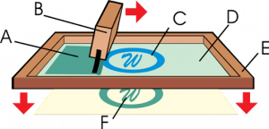
The stencils are negative images of the pattern for how the mask is to be applied to the circuit board. Stencils can be made in a variety of ways. Usually an image of the mask application pattern is photographed or photocopied and the photocopy is cut out and attached to the printing screen. In the photo-emulsion technique the screen is coated with a photographic emulsion. The masking pattern is drawn or attached to a transparent film and this film is laid over the emulsion-coated screen. The screen is then exposed to bright light. Everywhere that light passes through the photo-image, it strikes the emulsion causing the emulsion to harden and stick to the screen. The screen is then washed off which removes any photo-emulsion that was not exposed to the light and therefore did not harden. This creates an image of the masking pattern on the printing screen.
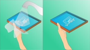
The prepared screen is then placed over the circuit board, liquid masking agent is then poured onto the screen and pressed through the screen with a rubber blade or squeegee. In this way the solder mask is placed on the circuit board in a sharply defined pattern. The printing process is then repeated with other circuit boards.
The printing screen can be re-used may times before it needs to be completely cleaned. Once use of the screen has been completed, the screen is cleaned completely to remove all traces of mask. The screen can then be stored for later use or the hardened photo-emulsion can be removed and the screen re-stenciled to create a completely different solder mask pattern.
The mesh size of the screen is important. The larger the mesh size, in relation to the particle size of the mask liquid being screen, the heavier the layer of mask that is applied to the circuit board. For the Chemask Water Filterable the largest particle size in on the order of 30 microns, which sets the limit of the screen holes when using this product. In reality larger screen sizes are used, to allow the application of a layer of mask sufficiently thick to completely shield all the parts of the boards when solder is not to be applied.
Screen sizes are quoted as the number of threads that cross within a square inch. As an example a 110 mesh screen has 110 threads crossing per each square inch of screen area. The more threads per each inch the smaller the holes in the screen material. The practical limit for the size of the holes will depend on the thickness or viscosity of the material being printed. The thicker the mask the greater the surface tension it has. More viscous materials are harder to press cleanly through the holes in the screen, so viscosity becomes a limiting factor in screen selection. Considering the viscosity of Chemask WF, screen sizes between 100 and 300 thread count are usually used, depending on the quality of the print detail required.
Selecting the right mesh size for the screen requires balancing the screen size against the viscosity of the mask, while taking into account the degree of fine detail that needs to be achieved in placing the mask on the board. The best mesh size to use must be determined by a few trial and error runs, starting with a particular mesh size, like 110, and then trying the same print pattern using a larger or smaller mesh size, as required to produce the detail desired. If the mesh size is too small the viscosity of the mask will prevent its movement through the holes in the screen. If the mesh size is too large, too much mask will be applied, which may result in spreading of the mask into areas of the board that should not be masked.
Since a squeegee or rubber blade is used to apply pressure to the mask liquid, to force it through the small holes in the screen and onto the circuit board, the screen printing method cannot be used to apply the Chemask peelable latex mask. The squeegee creates shearing forces as the mask is pressed through the screen. Putting shearing force on the Chemask peelable liquid causes the isoprene chains in the natural rubber latex to cross-link. This causes the mask to solidify immediately, which clogs the screen. This effect can be demonstrated by placing a drop of Chemask on a hard surface and smearing it with the fingertip; the mask will immediately solidify when force is applied.
Another complication with screening with peelable mask is the final clean-up. Uncured peelable mask can be washed away in a similar manner as Chemask WF. On the other hand, if cured, the only way to remove peelable mask is by peeling. That can be quite a challenge with a fine mesh screen or intricate stencil pattern.
If you need more technical information about this solution, do not hesitate to reach out with us through:
