
Embedded Flash (eFlash) memory is a key enabling technology for many programmable semiconductor products requiring small form factor and low-power processing. For example, microcontrollers use eFlash to store program instructions (code) as well as data on which processing is performed. The ability to update the code and data is essential.
IoT devices use eFlash to enable smart, flexible, and secure products that can be updated wirelessly, or over-the-air (OTA). Electronic devices with eFlash enable a wide-range of products from smart cards and wearables to factory automation systems and autonomous vehicles.
Infineon developed two different eFlash memory solutions, SONOS (Silicon Oxide Nitride Oxide Silicon) and eCT™ (embedded Charge Trap), to cover the application requirements from low-cost consumer to high-performance automotive. Both technologies are very compatible with CMOS and have been integrated into a foundry-standard logic processes while preserving CMOS device models and existing design IP.
Infineon uses these eFlash solutions in our microcontroller products (MCUs) for consumer, industrial and automotive markets. We’ve shipped billions of MCUs containing our eFlash technology over nearly two decades, demonstrating that our eFlash solutions are robust and proven. And, Infineon makes our eFlash solutions available for licensing to third-party companies.
Infineon’ SONOS is a patented and proprietary NOR Flash technology that was developed for cost-effective MCUs with low-power requirements. SONOS is a transistor with a polysilicon gate (S), an Oxide Nitride Oxide (ONO) gate dielectric, and a Silicon substrate (S) whose threshold voltage (Vt) can be changed by adding or removing electric charge from the nitride (ONO) layer. Infineon’ SONOS eFlash has been in production since 2001 on 350 nm and 130 nm nodes, and is now available on 65 nm, 55 nm, 40 nm and 28 nm nodes.
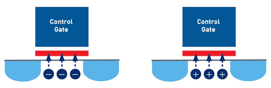
Infineon’ SONOS eFlash bit cell contains two transistors: a SONOS (Control Gate) and a MOS (Select Gate). One cell stores one bit of data for Flash or EEPROM.
The SONOS transistor is programmed by FN tunneling of electrons from the channel’s inversion layer through the bottom oxide of ONO and into traps within the nitride layer of ONO. It is erased by FN tunneling of holes from the channel’s accumulation layer into traps within the nitride layer of ONO.
The Infineon 55 nm and 40 nm SONOS eFlash macro families offer the most cost-effective, robust embedded Flash solutions for the next-generation 32-bit MCUs and IoT devices.
| SONOS eFlash | 55 nm | 40 nm |
|---|---|---|
| Cell Architecture | 2T, 1 bit/cell | 2T, 1 bit/cell |
| Density | 1 Mb, 2 Mb, 4 Mb, 8 Mb, 16 Mb | 1 Mb, 2 Mb, 4 Mb, 8 Mb, 16 Mb |
| Word Size | 32-bit | 32-bit |
| Output Bus Width | 32, 64, 128-bit | 32, 64, 128, 256-bit |
| Supply Voltage | 0.90 V – 1.32 V 1.62 V – 3.63 V |
0.81 V – 1.21 V 1.62 V – 3.63 V |
| Operating Temperature (Junction) | -40°C to +110°C | -40°C to +110°C |
| Read Access Time | 25 ns | 25 ns |
| Page Size | 4 kb | 4 kb / 8 kb |
| Page Programming Time (typ.) | 2 ms | 2 ms |
| Erase Sector Size | 1 Mb | 1 Mb / 2 Mb |
| Sector Erase Time (typ.) | 6 ms | 6 ms |
| Write Endurance | 100 k | 100 k |
| Data Retention | 10 years | 10 years |
| Extra Masks | 4 | 5 |
eCT™ is a patented and proprietary NOR Flash technology that Infineon developed for high-performance MCUs with stringent reliability requirements. eCT™ Flash is based on charge-trap technology that has been proven in volume production in six technology generations of MirrorBit® NOR Flash memory. eCT™ has been in volume production at the 40 nm node since 2016.
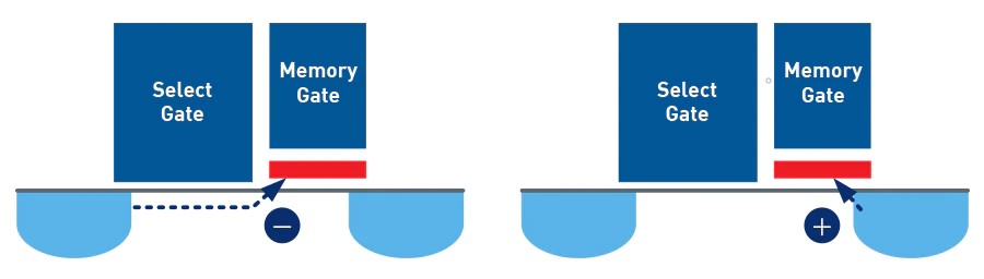
eCT™ Flash bit cell uses a split-gate (1.5T) architecture in which one transistor is a Memory Gate (MG) that stores non-volatile data, and the other is a Select Gate (SG). The threshold voltage (Vt) of MG can be changed by adding or removing the electric charge from the nitride layer of an Oxide Nitride Oxide (ONO) gate dielectric.
MG is programmed by channel hot electron injection (CHEI); Vt is increased by injecting electrons into traps within the nitride layer of ONO. The erase operation is accomplished by band-to-band tunneling (BTBT) hot hole injection. Vt is decreased by injecting holes into traps within the ONO nitride layer.
The Infineon 40 nm eCT Flash technology offers the most scalable high-performance, high-reliability embedded Flash solution for storing critical code and data with automotive reliability.
|
||||||||||||||||||||||||||||||||||||||||||||
The Infineon SONOS and eCT Flash process technologies are available for licensing to foundries. Under this license, Infineon transfers specific technology information to enable the integration of the embedded Flash technology into a specific logic or mixed-signal process for wafer manufacturing at the foundry. Infineon’ SONOS and eCT Flash technologies do not change any existing process design rules, device models or design IP. Infineon also works with foundries to provide all documentation necessary for a complete process design kit.
Infineon’ SONOS and eCT Flash design technologies are available for licensing to fabless semiconductor companies, IDMs, or foundries with design IP development teams. Under this license, Infineon transfers design information necessary for creation of new embedded Flash macro designs in Infineon’ SONOS or eCT Flash technologies by a customer’s design team.
Customers can also license our available off-the-shelf, silicon-validated SONOS or eCT macro designs. This option establishes the fastest path to market. Additionally, Infineon has a team of experienced engineers dedicated to providing custom Flash macro design services. In these cases, dedicated engineers consult with customer teams, engineer custom solutions and provide “design kit” Flash macros for integration into customer’s products.