Semiconductor, Printed Circuit Board, 5G Devices, Light-weight Electronic Devices.
- With the increasing number of wireless devices, designers are challenged with various electromagnetic, waves from multiple sources, radiating at the same spectrum of frequencies and resulting in electromagnetic interference (EMI).
- Radiofrequency (RF) emitting devices require effective isolation to limit the spread of their interference to neighboring components to protect the end device from performance degradation.
- As electronics move toward miniaturization, lighter weight, and higher speeds, these challenges become more significant as conventional shielding methods present functional and operational limitations.
Solution Range of EMI Shielding
Understanding the difficulties of engineers, PROSTECH is confident to introduce the two main solutions for EMI Shielding as below:
EMI Sealing for Entire Board
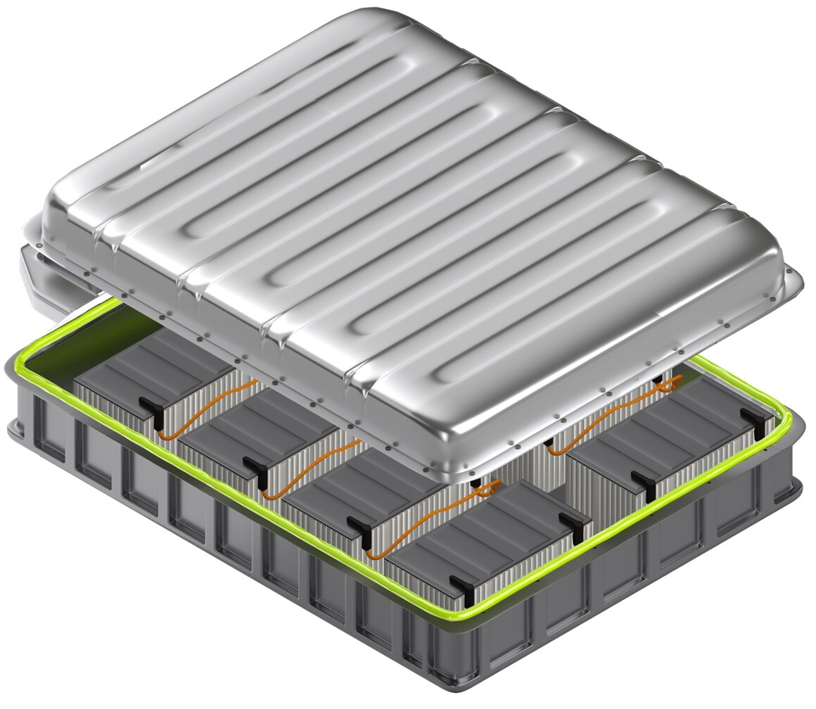
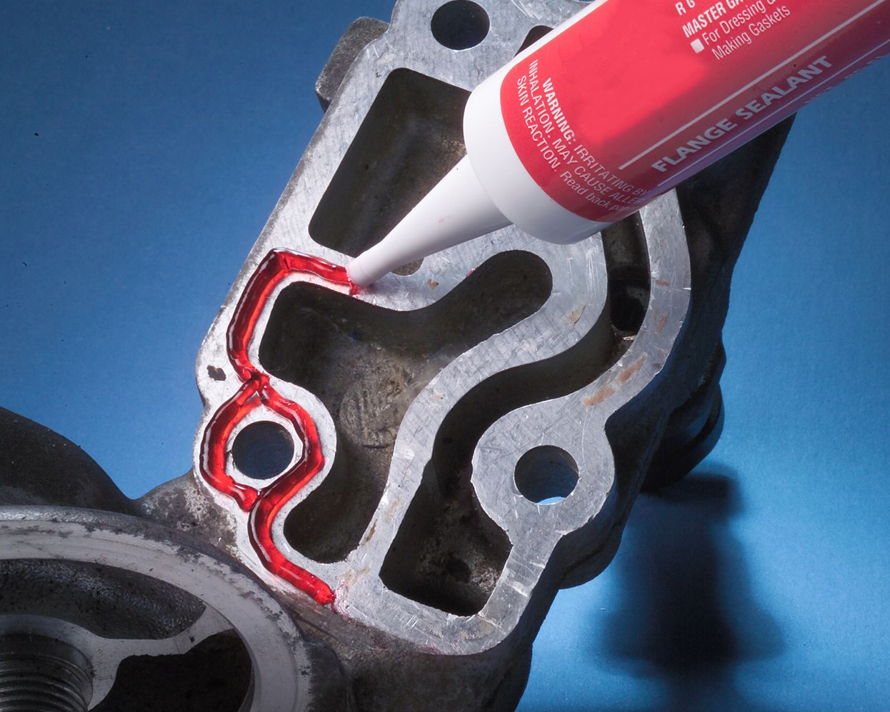
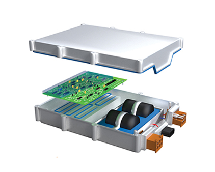
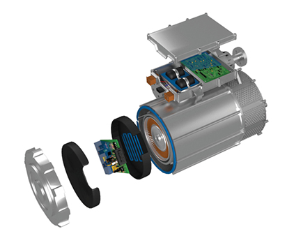
The method effectively used for several applications and industries, especially in large area sealing or bonding application as electric battery, big covers of motor and other equipment.
Basically, an electrically conductive adhesive (one part or two parts) will be used as a sealant or gasket material applied on the edge of the module’s covers. These adhesives are specially designed to be easily applied to panel joints/ seams and or the small clearances that result from non-continuous mechanical fixing in sheet metal enclosures.
Refer to some typical adhesive types here:
EMI Coating and Encapsulating on Semiconductor Package
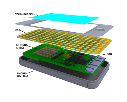
This EMI Shielding Method is an advanced solution for increasingly modern light-weight devices as smartwatch, 5G smartphone, tablet. Furthermore, this technology is used for almost all semiconductor level:
- Radiofrequency (RF)
- Wireless components
- Memory
- Sensors
- Other sensitive devices.
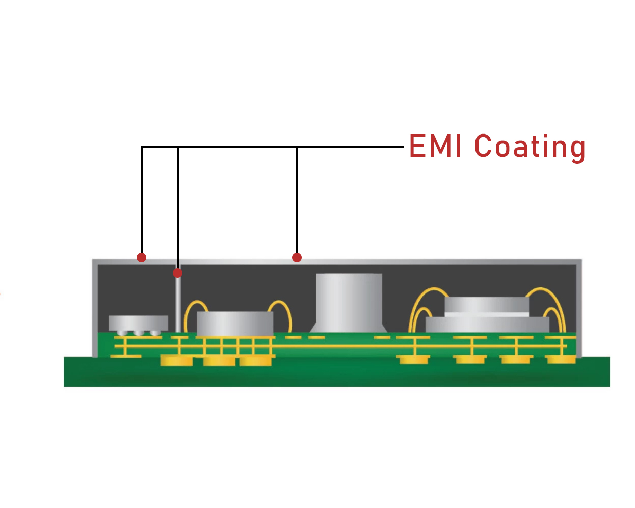
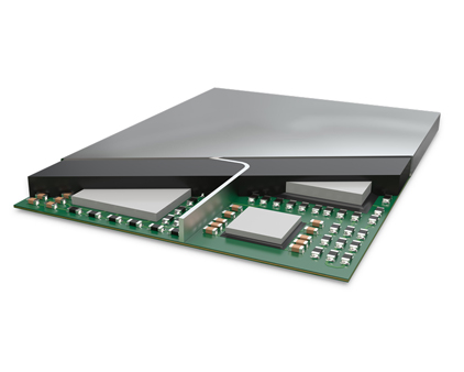
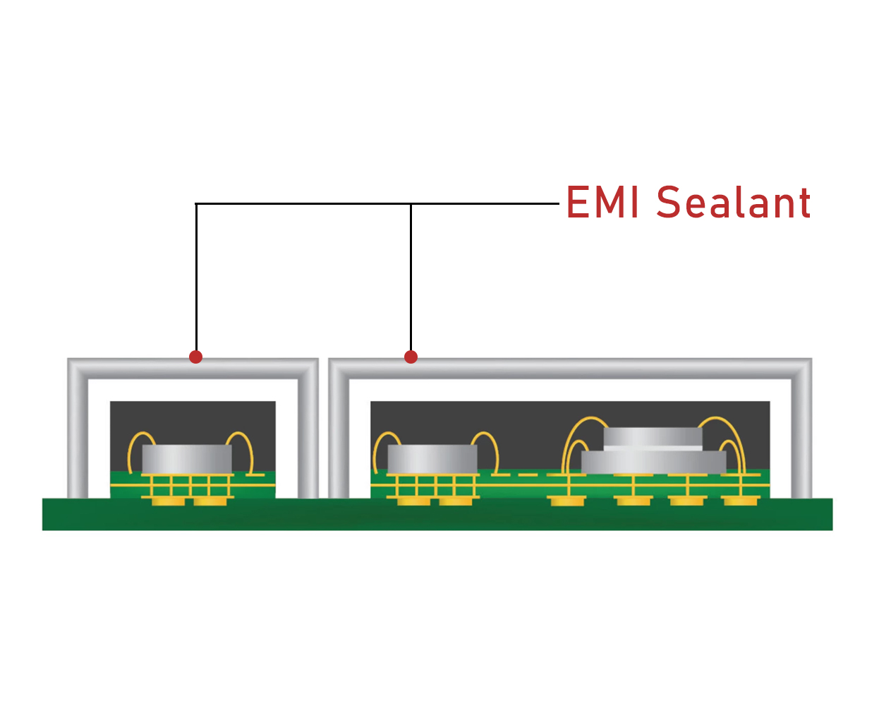
EMI Coating and Shielding on coverage of electronic module/ package
The thinly spray-coated material provides uniform coverage on top and sidewalls, clean edges without backside contamination, and excellent adhesion to mold compound with outstanding Shield Effectiveness (SE). This technology is simple, allowing easy production scalability and design flexibility with minimal cost of ownership using spray-coating, compared to other costly methods such as PVD/ sputtering.
| General Properties | EMI 8660S | EMI 8880S |
| Application Method | Spray | Spray |
| Viscosity, 5 rpm (cP) | 250 | 550 |
| Thixotropic Index (0.5 rpm/5 rpm) | 1.2 | 1.4 |
| Conductive Filler Type | Proprietary Ag | Proprietary Ag |
| Volume Resistivity (Ω∙cm) | 1.5 x 10^-5 | 7.9 x 10^-6 |
| Curing Condition | 175°C, 1 hour in air | 175°C, 1 hour in air |
| Optimal Coating Thickness (µm) | 3~5 | 3~5 |
| Adhesion to EMC (ASTM Cross Hatch Test) | 5B (0% peel) | 5B (0% peel) |
| Shielding Effectiveness (dB) | 90 (Excellent) | 90 (Excellent) |
| Target Frequency Range | 500 MHz ~ 10 GHz | 10 MHz ~ 10 GHz |
EMI Sealing and Shielding within one electronic component package
The jet-dispensed, highly flowable, conductive material can fill a narrow trench with high aspect ratios to create shielded partitioning within a package. This material technology offers high adhesion to the inner sidewalls and the bottom of the trench.
| GENERAL PROPERTIES | VALUE |
| Application Method | Jet-Dispense |
| Viscosity, 5 rpm (cP) | 5000 |
| Thixotropic Index (0.5 rpm/5 rpm) | < 1.5 |
| Conductive Filler Type | Ag or Ag-coated Cu |
| Volume Resistivity (Ω∙cm) | 7.0 x 10^-5 |
| Adhesion Interfaces | EMC, Copper, Solder |
| Supported Trench Width (µm) | 60 and above |
| Trench Aspect Ratio (Depth: Width) | Up to 10:1 |
| Cure Shrinkage | Low |
| Stress Management | Good |